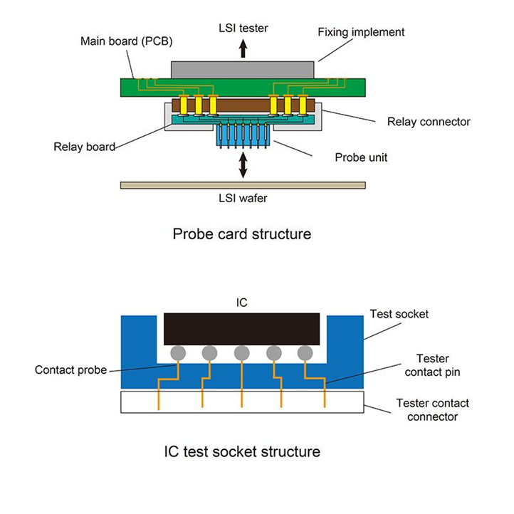
The semiconductor manufacturing process includes electrical testing steps that serve to ensure quality. These tests use probe cards and IC test sockets as electrode contact jigs. The former are used in wafer-level (upstream process) testing, while the latter are used in post-packaging (downstream process) testing. These components have multiple contact pins, and a defect affecting the contact reliability of even one pin will compromise the integrity of the test. As a result, manufacturers must test probe cards and IC test sockets to verify their reliability.
The semiconductor manufacturing process includes electrical testing steps that serve to ensure quality. These tests
use probe cards and IC test sockets as electrode contact jigs. The former are used in wafer-level (upstream process) testing,
while the latter are used in post-packaging (downstream process) testing. These components have multiple contact pins,
and a defect affecting the contact reliability of even one pin will compromise the integrity of the test. As a result,
manufacturers must test probe cards and IC test sockets to verify their reliability.
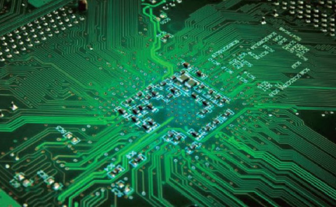
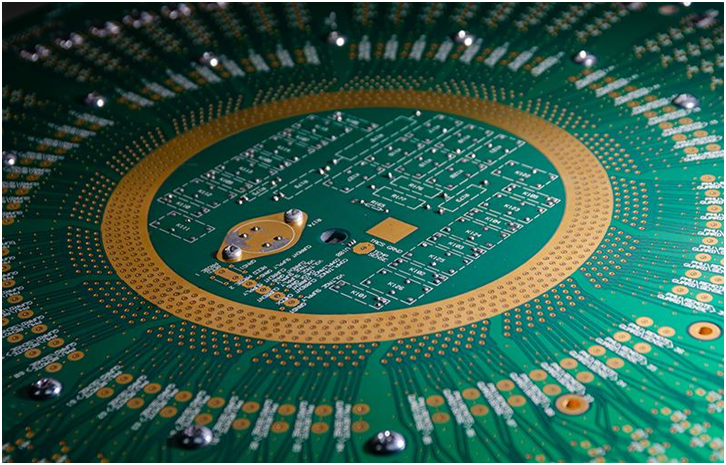
The IC test HDI PCB is one of the series HDI PCB developed and produced by Lingtech-PCB. This type of circuit board is made
of1000-2M material, manufactured by laser drilling, surface immersion and other processes, and the smallest
aperture can reach 0.1mm, the minimum line width and line spacing can reach 127/85um.
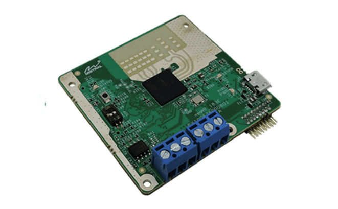
The HDI board is widely used in the field of IC testing.
thickness and hole diameter is 15:1.Long and short gold finger processing technology and high-density trace’s
precision control to meet the design requirements of photoelectric communication products.
product’s integrity requirements of signal transmission;
requirements of power products.
and meet the different levels of assembly requirements.
cost for customers under the premise of achieving the high-frequency performance of the products.
internal standard.
high-frequency material.
groove structure products.
tester and other reliability testing equipment to ensure product quality.